How Do Photonic Integrated Circuits Reduce Transceiver Cost?
How do photonic integrated circuits reduce transceiver cost? The short answer is that they replace a large collection of individually handled optical parts with a smaller number of repeatable, wafer-fabricated building blocks. In a conventional high-speed optical module, lasers, modulators, detectors, waveguides, filters, and monitoring components may each require separate packaging, alignment, testing, and interconnection. A photonic integrated circuit (PIC) brings many of those functions onto one platform.
That change matters most where bandwidth is rising faster than the industry’s tolerance for cost, power, and production complexity. Data center operators moving toward 400G, 800G, and higher interconnect speeds do not simply need more optical capacity. They need modules that can be built in volume, qualified consistently, repaired less often, and sourced without turning assembly lines into a precision-alignment bottleneck.
PICs do not make every transceiver automatically inexpensive. Their economic value depends on architecture, production scale, packaging strategy, yield, and the performance requirements of the application. But when those elements are aligned, photonic integration can reshape the cost structure of an optical transceiver rather than merely trimming the bill of materials.
The cost problem is often packaging, not just the optical chip
A transceiver is not priced only by the semiconductor die inside it. Its final cost includes optical components, electrical ICs, substrates, fiber attachment, thermal management, hermetic or semi-hermetic protection where needed, calibration, burn-in, functional test, yield loss, logistics, and warranty exposure. At higher data rates, each of these items becomes more demanding.
Discrete optical designs can be highly capable, especially in specialized or lower-volume applications. Yet they commonly require active alignment: technicians or automated equipment position fibers, lasers, lenses, and detectors while monitoring optical power until the required coupling efficiency is reached. Micron-scale tolerances make this work slow and sensitive. If one element is misaligned, a valuable partially assembled module may be lost.
Photonic integrated circuits attack this problem at its source. Instead of coupling a series of separate devices in free space or across multiple tiny subassemblies, the optical paths are lithographically defined on a chip. Waveguides route light between components with repeatable geometry. Splitters, multiplexers, phase shifters, modulators, and photodetectors can be designed as part of the same optical circuit.
The result is not “no packaging.” It is a shift from repeated component-by-component alignment toward fewer, more standardized packaging operations. That distinction is central for procurement teams evaluating the real cost potential of silicon photonics, indium phosphide PICs, or other integrated optical platforms.
Where PICs create savings across the transceiver value chain
1. Fewer discrete components and interfaces
Every separate optical component adds more than its purchase price. It adds incoming inspection, inventory management, handling risk, assembly time, attachment materials, and a potential failure point. A PIC can combine functions that would otherwise be sourced as separate parts: optical splitters, wavelength filters, Mach–Zehnder modulators, germanium photodiodes, variable optical attenuators, monitor taps, and passive waveguide routing.
In wavelength-division multiplexing designs, integration is especially valuable because multiple channels need controlled optical routing. A discrete approach may involve numerous filters and carefully assembled optical paths. An integrated multiplexer or demultiplexer can replace much of that optical plumbing. The module becomes physically simpler even if the design and fabrication of the chip are more sophisticated.
2. Lower active-alignment burden
Active alignment is one of the quiet cost drivers in optics manufacturing. It consumes equipment time, requires accurate feedback systems, and can complicate automation. PIC platforms can support approaches such as edge coupling, grating couplers, fiber arrays, and passive alignment features that reduce the number of delicate positioning steps.
Passive alignment is not universally easy, and coupling losses must still be controlled. However, when a platform is designed around standardized optical interfaces, factories can use fixtures, v-grooves, alignment marks, and automated placement techniques more effectively. The benefit becomes increasingly visible when modules are produced in high volume.
For a transceiver manufacturer, the important question is not merely whether a PIC uses fiber coupling. Nearly every optical module does. The more useful question is: how many critical alignments must be completed, how tight are their tolerances, and can they be executed reliably with a scalable assembly process?
3. Wafer-scale manufacturing and test opportunities
Discrete photonic assembly grows largely one module at a time. PIC fabrication introduces wafer-scale economics. Hundreds or thousands of devices can be patterned through standardized semiconductor processes, and many circuit features can be inspected before the wafer is diced.
Wafer-level electrical probing, optical test structures, and process-control monitors help manufacturers identify variation earlier. A defective die can be screened before expensive package assembly begins. That does not eliminate all downstream failures, but it reduces the chance of investing laser attach, fiber attach, driver integration, and final test time into a device with an underlying photonic defect.
Scale is important here. A custom PIC with modest demand can carry high non-recurring engineering expense, mask costs, process-development overhead, and limited wafer utilization. By contrast, a mature platform serving common data center or telecom configurations can spread those costs over far more units. PIC economics are strongest when standardization and shipment volume meet.

4. More compact modules with fewer mechanical compromises
As port density rises in switches and routers, physical space becomes part of the cost equation. A compact optical engine can reduce the need for complex internal mounting structures, long optical paths, or multiple miniature subassemblies. It may also simplify the route from the electrical interface to the optical interface.
Smaller does not always mean cooler. Dense integration can concentrate heat, and thermal design remains a serious engineering task. Still, a more compact architecture can reduce enclosure complexity and support denser front-panel configurations. For hyperscale and cloud data center environments, the system-level value of fitting more bandwidth into a constrained space can be substantial, even when the module-level price reduction is moderate.
5. Better consistency can improve yield and reliability economics
Manual assembly variation is expensive because it appears in several places: optical power variation, extinction ratio drift, return-loss problems, calibration time, and early-life failures. Lithographic fabrication does not remove variation, but it can make the optical geometry more controlled and repeatable than an assembly made from many separate aligned parts.
Integrated monitor photodiodes, thermal tuning elements, and control loops can also help maintain operating conditions over temperature and aging. These features add design complexity and may increase chip area, yet they can reduce costly performance scatter at the finished-module level. A transceiver that is easier to calibrate and more predictable in the field has a lower total cost of ownership than one that is merely inexpensive at factory exit.
A practical comparison: discrete optics versus an integrated optical engine
The difference is best understood as a manufacturing model rather than a contest between “old” and “new” technology. Discrete optics remain appropriate for unusual wavelengths, extreme optical power, low-volume instruments, or architectures that demand individually optimized components. PICs are most compelling when a repeatable function must be delivered many times.
Laser integration is valuable, but it is not the only path to lower cost
One common misunderstanding is that a PIC must integrate the laser to be economically useful. Laser integration can reduce component count and simplify optical coupling, particularly on indium phosphide platforms where active devices and waveguides can be integrated monolithically. It can be attractive for certain coherent transceivers and dense wavelength-channel architectures.
Yet laser integration introduces its own challenges: thermal sensitivity, yield management, linewidth requirements, optical isolation, and the need to optimize active and passive functions on the same process. In some silicon photonics transceivers, an external laser source is coupled to the photonic chip. This hybrid arrangement can preserve some advantages of integration while allowing laser performance, sourcing, or reliability strategy to be managed separately.
The right architecture depends on what is driving the cost. If fiber attach and passive optical complexity dominate, a silicon photonics PIC with external lasers may still deliver a compelling reduction. If separate laser subassemblies are the principal source of cost and variation, deeper integration may be justified. There is no universal winner; the target application decides.
Why 800G economics place more pressure on integration
At lower speeds, manufacturers can sometimes absorb the inefficiency of a more component-heavy architecture. As lane rates increase, signal integrity, bandwidth, power consumption, and thermal margins become less forgiving. More electrical lanes, more optical channels, or more complex modulation formats can quickly multiply the number of interfaces that must perform correctly.
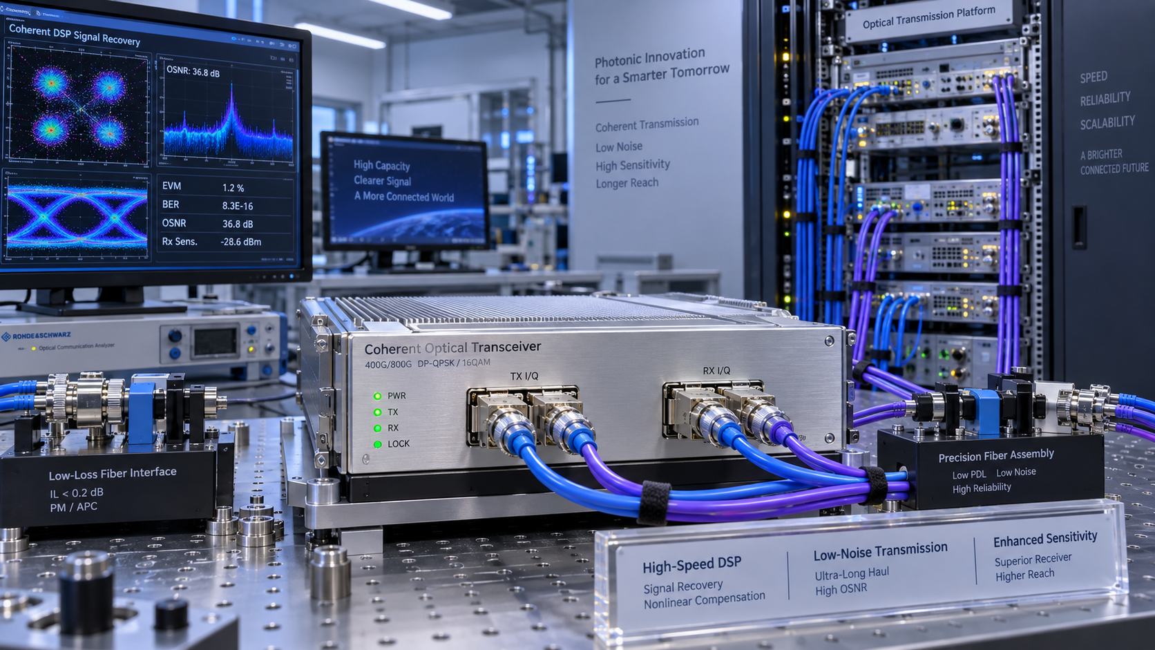
This is why PICs are closely associated with 400G, 800G, coherent pluggables, and future high-density optical interconnects. Integration enables a controlled optical path between modulators, multiplexers, detectors, and monitor functions. It also supports co-packaged optics discussions, where the electrical distance between switching silicon and optical engines is reduced to address high-speed electrical loss and power concerns.
Still, module buyers should avoid treating “PIC-based” as a complete specification. A cost-effective 800G design must balance photonic architecture with driver and transimpedance amplifier performance, packaging yield, host compatibility, forward error correction requirements, thermal behavior, and serviceability. The PIC is an important lever, not the entire system.
What can prevent a PIC from delivering the expected savings?
Integration concentrates risk as well as function. A design flaw in one critical building block can affect the entire chip. Larger die area may reduce die-per-wafer count and expose the manufacturer to higher yield sensitivity. A sophisticated package involving high-frequency electrical connections, laser coupling, thermal control, and fiber-array attachment can remain expensive even when the photonic circuit itself is elegantly integrated.
Another risk is over-customization. A bespoke PIC can be technically impressive but commercially difficult if only a small number of customers use the exact wavelength plan, connector arrangement, or form factor. Platform reuse matters. Suppliers that share validated building blocks across several module families are generally better positioned to convert integration into manufacturing savings.
There is also a supply-chain consideration. Some PIC ecosystems depend on specialized foundries, packaging houses, laser suppliers, or proprietary process design kits. Buyers should assess second-source options, lead times, qualification ownership, and the availability of failure-analysis support. A lower nominal unit cost is less valuable if the supply chain is fragile.
A buyer’s checklist for evaluating PIC-based transceivers
For engineering leaders, procurement managers, and product planners, the most useful evaluation goes beyond asking whether a supplier uses silicon photonics or indium phosphide. Request evidence of how the architecture changes the manufacturing flow.
- Which optical functions are integrated, and which remain discrete?
- How many active alignment operations are required during assembly?
- Can critical photonic parameters be tested at wafer level before packaging?
- What are the key yield limiters: die fabrication, laser attach, fiber coupling, RF packaging, or final calibration?
- How does the design manage temperature, wavelength drift, and optical power monitoring?
- Is the platform reused across multiple transceiver products, or is it highly customized?
- What packaging partners, foundry routes, and component sources support continuity of supply?
These questions reveal whether the claimed cost advantage comes from a scalable industrial process or simply from a compact technical demonstration. In optical communications, manufacturability is inseparable from performance.
The larger economic case: cost per transported bit
The most meaningful metric is often not the purchase price of a single transceiver. It is the cost per transported bit over the life of a network. A PIC-based module may justify its place through a combination of lower assembly cost, reduced power per bit, higher port density, more consistent performance, and fewer operational interventions. In some deployments, these system benefits outweigh a small difference in initial module price.
For optical component producers, PICs offer a route to repeatable product platforms. For data center operators, they offer a way to pursue bandwidth growth without allowing optical assembly complexity to rise at the same rate. For telecom equipment makers, integrated photonics can support denser coherent architectures while creating opportunities for more disciplined testing and supply-chain planning.
Ultimately, photonic integrated circuits reduce transceiver cost by making optics more manufacturable. They turn delicate optical functions into circuits that can be fabricated, measured, packaged, and scaled with greater consistency. The savings are real when the design is matched to volume, packaging is engineered as carefully as the chip, and the supplier has converted integration into a stable production platform rather than a promising laboratory concept.
Recommended News
 Area Scan CamerasHow Multispectral Imaging Inspection Detects Defects Beyond RGB VisionMultispectral imaging inspection detects hidden defects beyond RGB vision, revealing moisture, oil, coating variation, and material differences for smarter quality control.Oct 04, 2026Author:Machine Vision Optical Expert
 Opto-Capital & Vision EconOptical Component Vendor Qualification: A Risk-Based Checklist for Procurement TeamsOptical component supply chain vendor qualification: use a risk-based checklist to assess quality controls, traceability, production continuity, and sourcing risk.Oct 03, 2026Author:Mr. Orion Cross
 Narrowband/IR Cut FiltersOptical Filter Durability: Choosing Dielectric Thin-Film MaterialsDielectric thin film materials determine optical filter durability. Explore how material pairs, deposition quality, substrates, and validation protect spectral performance in demanding environments.Oct 02, 2026Author:Optical Coating Scientist
 Silicon Photonics OPAPhotonic Sensor Design for LiDAR: Key Trade-Offs in Range, Resolution, and CostPhotonic sensor design for LiDAR: explore the critical trade-offs in range, resolution, wavelength, receiver performance, and cost for reliable, scalable sensing systems.Oct 01, 2026Author:LiDAR Systems Fellow
 Optical TransceiversOptical DSP Algorithms: Improving Receiver Sensitivity in Coherent TransceiversDSP algorithms optics improve coherent transceiver receiver sensitivity through dispersion compensation, polarization equalization, phase recovery, and FEC—assess reach, OSNR, and link margin.Sep 30, 2026Author:Photonics Strategist
 Non-linear Optics & ThermalSelecting Low-Loss Infrared Optical Components for High-Power Laser SystemsInfrared optical components low loss: learn how to select materials, coatings, and mounts that protect beam quality, reduce thermal risk, and improve laser uptime.Sep 29, 2026Author:Prof. Kaelen Sterling
 Area Scan CamerasWhat to Evaluate When Sourcing Optoelectronic Sensors for German Factory AutomationOptoelectronic Sensors Germany: learn how to evaluate detection reliability, PLC and IO-Link integration, environmental protection, lifecycle cost, and supplier support for dependable factory automation.Sep 28, 2026Author:Machine Vision Optical Expert
 Area Scan CamerasSelecting Industrial Automation Imaging Cameras for High-Speed Inspection LinesIndustrial automation imaging camera selection guide for high-speed inspection lines—compare resolution, shutters, lighting, optics, and data flow for reliable defect detection.Sep 27, 2026Author:Machine Vision Optical Expert
 PM & Radiation-hard FibersHow Submarine Optical Cables Are Designed to Withstand Deep-Sea Pressure and FaultsSubmarine optical cables are engineered to withstand deep-sea pressure, route hazards, and faults. Explore layered protection, monitoring, and repair strategies.Sep 26, 2026Author:Photonics Strategist
 3D Laser ProfilersTime-of-Flight Technology Standards: Accuracy, Safety, and Interoperability RequirementsTime-of-flight technology standards explained: compare accuracy, laser safety, functional safety, and interoperability requirements for reliable ToF deployment.Sep 25, 2026Author:Machine Vision Optical Expert
 3D Laser ProfilersBeam Diagnostics for M² Measurement: Methods, Accuracy Limits, and Setup ChoicesBeam diagnostics M2 measurement explained: compare ISO-aligned methods, accuracy limits, and setup choices to qualify lasers, reduce risk, and improve optical performance.Sep 24, 2026Author:Machine Vision Optical Expert
![]() Opto-Capital & Vision EconWhat Should Be Checked Before Accepting a Precision Optical Component?What should be checked before accepting a precision optical component? Explore essential checks for geometry, surface quality, coatings, materials, traceability, and documentation.Sep 24, 2026Author:Mr. Orion Cross
Opto-Capital & Vision EconWhat Should Be Checked Before Accepting a Precision Optical Component?What should be checked before accepting a precision optical component? Explore essential checks for geometry, surface quality, coatings, materials, traceability, and documentation.Sep 24, 2026Author:Mr. Orion Cross![]() Optical TransceiversHow Do Photonic Integrated Circuits Reduce Transceiver Cost?How do photonic integrated circuits reduce transceiver cost? Explore how PICs cut alignment, packaging, and scaling costs for high-speed optical modules.Sep 24, 2026Author:Photonics Strategist
Optical TransceiversHow Do Photonic Integrated Circuits Reduce Transceiver Cost?How do photonic integrated circuits reduce transceiver cost? Explore how PICs cut alignment, packaging, and scaling costs for high-speed optical modules.Sep 24, 2026Author:Photonics Strategist![]() Silicon Photonics OPAIs Silicon Photonics Ready for High-Volume Optical Transceivers?Is silicon photonics ready for high-volume optical transceivers? Explore its 800G potential, packaging challenges, cost drivers, yield, and buyer-ready decision factors.Sep 24, 2026Author:LiDAR Systems Fellow
Silicon Photonics OPAIs Silicon Photonics Ready for High-Volume Optical Transceivers?Is silicon photonics ready for high-volume optical transceivers? Explore its 800G potential, packaging challenges, cost drivers, yield, and buyer-ready decision factors.Sep 24, 2026Author:LiDAR Systems Fellow![]() Non-linear Optics & ThermalHow Do Optical Materials Affect Laser Damage Resistance?How do optical material choices affect laser damage resistance? Explore absorption, coatings, thermal stress, and material selection for reliable high-power laser optics.Sep 24, 2026Author:Prof. Kaelen Sterling
Non-linear Optics & ThermalHow Do Optical Materials Affect Laser Damage Resistance?How do optical material choices affect laser damage resistance? Explore absorption, coatings, thermal stress, and material selection for reliable high-power laser optics.Sep 24, 2026Author:Prof. Kaelen Sterling![]() Narrowband/IR Cut FiltersWhich Optical Coating Is Best for Stray Light Suppression?Which optical coating is best for stray light suppression? Compare broadband AR, V-coatings, and black absorptive finishes to improve contrast, reduce flare, and protect system performance.Sep 24, 2026Author:Optical Coating Scientist
Narrowband/IR Cut FiltersWhich Optical Coating Is Best for Stray Light Suppression?Which optical coating is best for stray light suppression? Compare broadband AR, V-coatings, and black absorptive finishes to improve contrast, reduce flare, and protect system performance.Sep 24, 2026Author:Optical Coating Scientist![]() PM & Radiation-hard FibersWhen Should a Fiber Optic Sensor Be Replaced?When should a fiber optic sensor be replaced? Learn the warning signs, from signal drift and unstable switching to damage, calibration failure, and lost optical margin.Sep 24, 2026Author:Photonics Strategist
PM & Radiation-hard FibersWhen Should a Fiber Optic Sensor Be Replaced?When should a fiber optic sensor be replaced? Learn the warning signs, from signal drift and unstable switching to damage, calibration failure, and lost optical margin.Sep 24, 2026Author:Photonics Strategist![]() 3D Laser ProfilersHow Accurate Is Time-of-Flight Sensing for Industrial Measurement?How accurate is Time-of-Flight sensing for industrial measurement? Explore real-world accuracy factors, applications, and validation tips for reliable ToF performance.Sep 24, 2026Author:Machine Vision Optical Expert
3D Laser ProfilersHow Accurate Is Time-of-Flight Sensing for Industrial Measurement?How accurate is Time-of-Flight sensing for industrial measurement? Explore real-world accuracy factors, applications, and validation tips for reliable ToF performance.Sep 24, 2026Author:Machine Vision Optical Expert![]() FMCW Laser SourcesIs 1550 nm LiDAR Better for Long-Range, Low-Light Sensing?Is 1550nm LiDAR better for long-range low-light sensing? Explore eye-safe power, range potential, detector trade-offs, weather limits, and how to choose the right LiDAR architecture.Sep 24, 2026Author:LiDAR Systems Fellow
FMCW Laser SourcesIs 1550 nm LiDAR Better for Long-Range, Low-Light Sensing?Is 1550nm LiDAR better for long-range low-light sensing? Explore eye-safe power, range potential, detector trade-offs, weather limits, and how to choose the right LiDAR architecture.Sep 24, 2026Author:LiDAR Systems Fellow![]() Telecentric LensesWhat Causes Distortion in Industrial Machine Vision Lenses?What causes distortion in industrial machine vision lenses? Discover key optical, sensor, and setup factors—and how to improve inspection accuracy.Sep 24, 2026Author:Machine Vision Optical Expert
Telecentric LensesWhat Causes Distortion in Industrial Machine Vision Lenses?What causes distortion in industrial machine vision lenses? Discover key optical, sensor, and setup factors—and how to improve inspection accuracy.Sep 24, 2026Author:Machine Vision Optical Expert